Thank you so much for digging and for coming back on this. Very much appreciated!
Also for coming back at all, as I am just some random nerd at this time, obviously not some “big fish” with big numbers of PCBs coming around;)
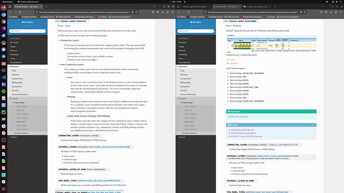
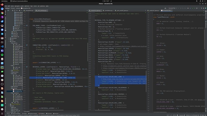
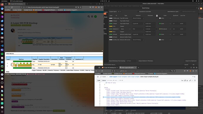
So according to the datasheet, and the other information on the stackup, the 2-layer AISLER stack has a dielectric layer with
- Thickness (processed) 1550um
- Permittivity 4.7
- Loss Tangent 0,020
I will add this information into my modeling code.
Obviously, having consistent information in the AISLER docs would be nice and great as well 
Now, I am still “getting into” all of this, and gain experience, try out different tools, methods and also manufacturers, both PCB and PCBA, and for the different boards my device needs.
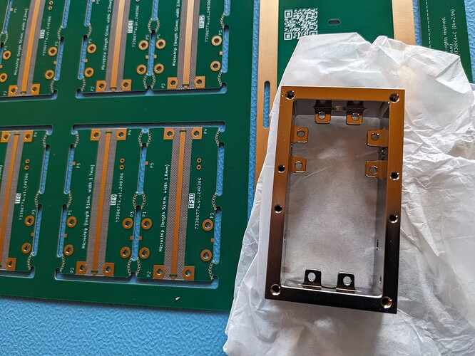
FWIW, for the antenna boards, I now have ready made first PCBs from a different source which I will use to validate / calibrate my openEMS models:
I haven’t done assembly and VNA measurements yet, so I should be careful, but for the antenna boards of my device (and those are just one of two types I need), above looks good - it’s using low Dk PTFE.
I will come back once I target the mentioned 2nd board type for the device, which will likely use a more “standard” 4-layer FR4, and PCBA is crucial for that as well, and I’d love to give that a try via AISLER!
thanks again, kind regards,
/Tobias


