How long does it take to manufacture and transport for 2 layer complex board, if I order 2-3 same boards (without Mounting or Assmbly)? My location is Germany.
Thanks ![]()
It will take 8 Business days at most, please note that this is impacted by holiday days.
For more information, have a look at our Service Status and Shipping documentation.
Thank you very much. And I have some futher questions about design rules. In PCB Design Rules there are already many needed rules but in kicad there is one constraints called ‘‘Minimum connection width’’, which value should I set here ?
![]()
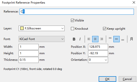
And also I didn’t find any rules about footprint reference, is there any constraints about the text (width, height, thickness …) ?
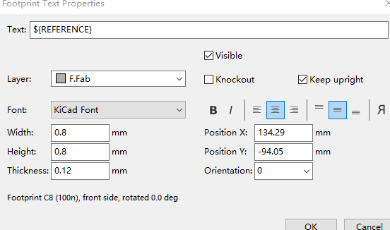
Last, there is some content belong to layer ‘’ F.Fab’', which shows the value of each components, should I do somthing about it ?
Footprint Reference:
Footprint Text(F.Fab):
I am using Kicad btw ![]()
Hi,
The minimum connection width should be at least the minimum track width, but we recommend a larger width than the minimum when connecting large copper planes.
You can find more information about the text height requirements in our Silkscreen Specification.
We don’t use the F.Fab layer to manufacture bare PCBs so you can safely ignore it.